Waveguide Technology Innovations: The Story of the Invention (And Reinvention) of TriPleX®
In the world of photonic integrated circuits, as in many other science and engineering fields, the eureka moments often arise from persistence and coincidence. Our silicon nitride waveguide technology, TriPleX®, is no different. This is the story of how it came about almost exactly 20 years ago, and how it remains a silicon nitride platform that rivals all others in stability and maturity today.
“TriPleX ® is a simple yet powerful solution that unlocks the full potential of silicon nitride layers. Reproducible and cost-effective in larger batches—truly a game-changer!” René Heideman, CTO LioniX International
The story started with an atypical request. Nowadays, LioniX International deals with a lot of these, since our work is completely custom. But back in 2003, one customer made a seemingly simple request, at least at first: a 600 nm thick high index waveguiding material. While we were looking at three materials of waveguides: LPCVD silicon-rich nitride (SiRN), PECVD silicon oxynitride (SiON) and PECVD silicon nitride (to be deposited on thermally grown silicon dioxide), the client thought that we would be using LPCVD silicon nitride.
However, at the time, no one had made such a layer thicker than 350 nm without it cracking and ruining the waveguides. We then went back to the drawing board and came up with the idea of using a stack approach and introducing a layer of LPCVD TEOS silicon dioxide to reduce stress and overcome the thickness limit, because the type of stress in the two materials is opposing, tensile versus compressive. Let them cancel each other out! This was the first time when someone used a layer stack approach based on LPCVD silicon nitride to overcome its critical layer thickness limitation.
Figure 1: Marcel working on perfecting TriPleX ® technology back in December 2005
Taking a wafer from another project, the team made waveguides in 220 nm LPCVD silicon nitride. On top of this, we first deposited a layer of 250 nm LPCVD TEOS silicon dioxide then another layer of 220 nm LPCVD silicon nitride. The results exceeded expectations, overcoming the technological barrier with no cracks and finding unexpectedly low propagation losses compared to the original waveguide.
“Marcel and I independently arrived at the same solution, a moment that hit me like a bolt of lightning!” René Heideman, CTO LioniX International
This success paved the way for the development of stable waveguide technology, leading to the formulation of TriPleX® patents.
Evolution of Waveguide Configurations: From Box-Shaped to Asymmetric Double-Stripe
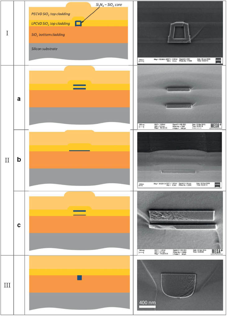
During the first years the focus was on a box-shaped waveguide—a silicon nitride box around a rectangular silicon dioxide core— suitable for telecom applications. While offering polarization independence, the complexity of manufacturing and time consumption posed challenges in meeting Telcordia specifications (or the requirements that have to be fulfilled for telecommunication devices).
In 2012, LioniX international started offering Infrared Multi-Project Wafer (IR-MPW) runs based on the box-shaped waveguide. A year later, the shift towards a double-stripe configuration took place. If in the beginning we chose to work with waveguides with same thicknesses, consisting of two stripes of silicon nitride, vertically separated by and covered with silicon dioxide. It soon became clear that making layers at different thicknesses could offer a high spectrum of possibilities and simplify the manufacturing process. We called the waveguides with same thickness symmetric double stripe (SDS) and the ones with different thicknesses asymmetric double-stripe (ADS).
The thickness of the bottom stripe has been optimized for low loss coupling to glass fibers and gain sections. We also developed a vertical taper, enabling the smooth removal of the top stripe for making low-loss spot-size converters—an essential innovation during the time when we used contact lithography for defining waveguides.
By optimizing the two silicon nitride layers independently, it was possible to optimize the bottom layer for good coupling to peripherals (glass fibers, gain section chips, etc.). The top layer was optimized for giving the waveguide a small bending radius, which allowed for very large-scale integration of photonic devices (VLSI photonics). Because of improvement of minimum feature size, local removal of the top stripe for spot-size converters (SSCs) was not required anymore: everything could be defined using the complete layer stack.
TriPleX® nowdays: Redefining Photonic Integration
After a long journey paved with challenges, TriPleX® evolved into a mature and stable silicon nitride waveguide technology. Characterized by extremely low propagation losses, ranging from 0.1 dB/cm down to an impressive 0.1 dB/m, it becomes ideal for applications across a broad wavelength band from 405 nm to 2350 nm.
With versatile waveguide structures including box shapes, single stripes, symmetric double stripes (SDS), and asymmetric double stripes (ADS), TriPleX® offers tailored properties for specific applications. The asymmetric double stripe (ADS) serves at 1550 nm applications, boasting losses below 0.1 dB/cm and fiber coupling losses below 0.5 dB per facet with a spot size converter. Meanwhile, the single stripe version excels in ultra-low loss applications, operating within the visible light domain with minimal losses.
TriPleX® embraces hybrid integration, enhancing functionality by enabling seamless integration with various components for light generation, modulation, and detection. Applications span integrated optical beamforming and filtering modules, hybrid integrated tunable lasers, optical phased arrays, and integrated biosensor chips.
Figure 2 : Schematics and corresponding SEM images of different TriPleX waveguide cross sections.

Marcel Hoekman studied Applied physics at the University of Twente and graduated at the Integrated Optical Micro Systems group in 1998. In 2001 he finished a post graduate design program within the same group, based on the design of an integrated optical electro-optical modulator based on PZT containing multilayer-stacks, working together with Radboud University Nijmegen. From 2004 to 2009 he has been a part-time PhD student at the Integrated Optical Micro Systems group of the University of Twente. In 2001 he joined LioniX as a design engineer. Besides simulation and mask design, he has experience in several cleanroom manufacturing processes and characterization methods, and he has worked as project leader on several projects.


