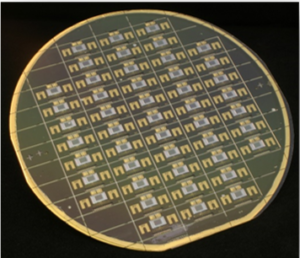
MEMS Wafer-Level Packaging
Wafer level packaging for MEMS mitigates against potential disruption of mechanically fragile mems devices. This is especially valuable where MEMS contain fragile mechanical structures such as cantilevers and accelerometers.
The packaging process involves bonding a capping wafer to the MEMS wafer before dicing. This provides a stable and hermetically sealed environment for robust MEMS performance. In addition, MEMS packaging can be used to incorporate functional elements such as sensing windows.
This type of MEMS packaging is carried out as part of wafer-level manufacturing process and so is known as wafer level packaging. The MEMS technology is also referred to as 3D packaging.
MEMS Packaging: Wafer bonding capabilities
We choose specific packaging methods to your requirements, taking into account the required operating parameters of your MEMS device. Our available capabilities include:
- Vacuum bonding
- Hermetic bonding
- Cavity bonding
- Aligned bonding
- Chemical mechanical polishing (CMP)
Wafer bonding processes
Our range of wafer bonding processes for wafer level packaging are suitable for silicon wafer bonding as well as the bonding of other materials such as metals and glass. Using appropriate methods, we optimise performance and cost and ensure MEMS are protected during packaging and function.
Available bonding processes include:
- Direct bonding
- Anodic bonding
- Thermocompression bonding
- Eutectic bonding
- Epoxy bonding
- BPSG bonding

