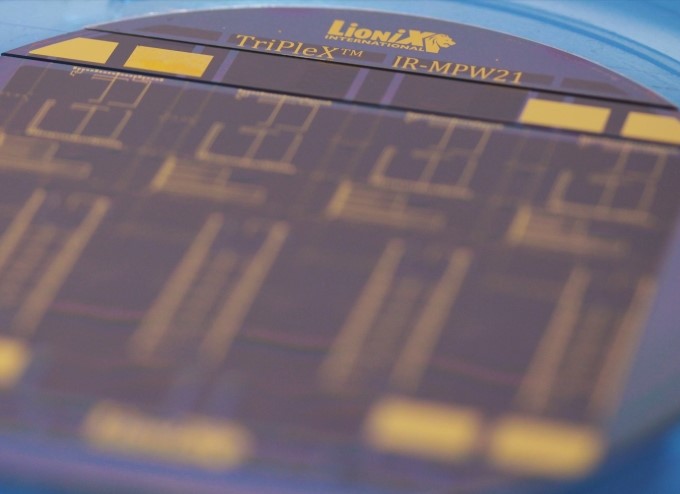
Benefit from very low propagation loss across a very broad wavelength range with TriPleX® silicon nitride waveguides.
Multi project wafer runs are particularly useful when you:
- Are exploring integrated photonics’ possibilities.
- Have an idea in the research phase.
- Just need a few chips for your design.
- Are investigating what technology fits your application.
- Are looking for the lowest entry costs.

“We were excited to access silicon nitride technology through the LioniX International MPW. Our application required really low-loss photonics in chip volumes appropriate to our early-stage technology. The design tools and building-blocks gave us and our partners an efficient way of doing the functional design and the packaging services saved us valuable time on our end.”

“As a developer of PIC based products for third parties, Bright Photonics has seen a predictable and very good performance from LioniX MPW run PICs over the last years, which makes it an excellent platform for SiN prototyping for us.”
Additional multi project wafer services
We recognize that you might want more than just your design fabricated on a chip. Thus, even in our multi project wafer program, we let our vertically integrated process add extra bang for your buck. Here’s the rundown:
- Our process design kit (PDK) is available through different design platforms from Synopsys, Nazca, and Luceda.
- You get access to training for our design tools and additional design support.
- Additional post-fabrication steps are available on request, including trench etching for heat localization and fluidics, glass bonding, and fluidic connections.
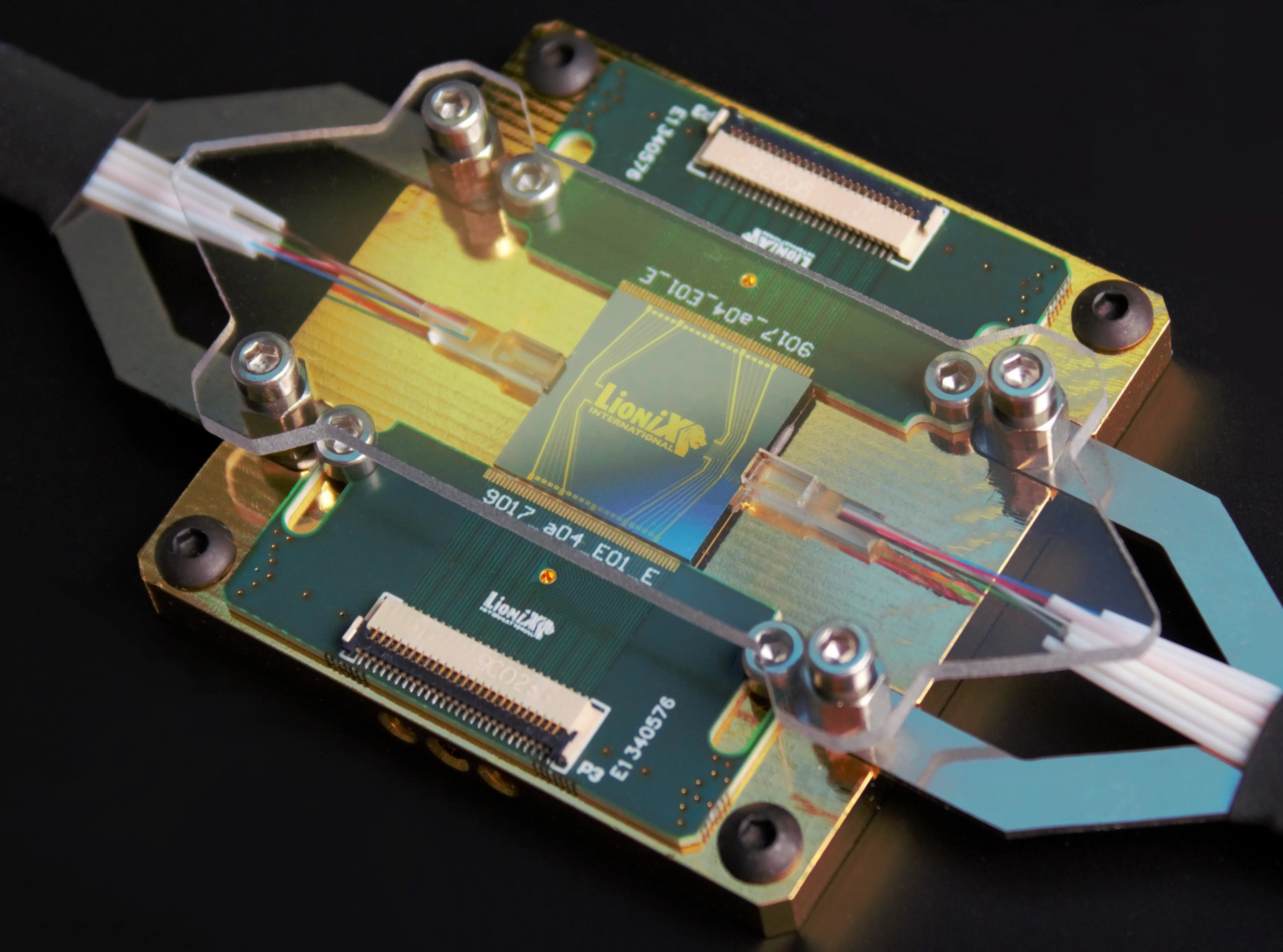
- You can make use of our expertise in fiber coupling and electronics design in our cost-effective packaging solution: the Characterization and Packaging Service (CPS).


