scalable quantum computing with a photonic integrated ion trap
A photonic integrated ion trap fabricated by LioniX International has been used to create a scalable building block for quantum computing rivalling the most sophisticated experiments. The ion traps, described in a publication in the journal Nature1, were designed by a team at ETH Zurich for use in quantum computing to create “qubits”, the quantum equivalent of the “bit” in classical computing.
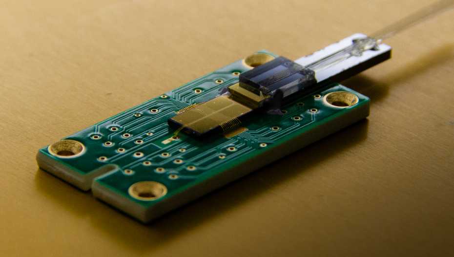
The completed ion trap chip with electrical and optical interfaces added by the team at ETH. Photograph: K. Mehta / ETH Zurich
A photonic integrated ion trap fabricated by LioniX International has been used to create a scalable building block for quantum computing rivalling the most sophisticated experiments. The ion traps, described in a publication in the journal Nature1, were designed by a team at ETH Zurich for use in quantum computing to create “qubits”, the quantum equivalent of the “bit” in classical computing.
A central challenge in quantum computing remains the creation of low-noise qubits that can be scaled to sufficiently high numbers for useful computation. One contender for a viable quantum processor uses lasers to manipulate the very fragile quantum states of trapped ions in a super-cooled vacuum environment. But this approach relies on the extremely careful alignment of free-space optics to deliver light within cryogenic and vacuum environments. The inherent noise involved in such an approach and the need to carefully configure optical systems for each qubit are major barriers to scaling.
Custom fabrication for scalable solutions
To address barriers to scaling, the research team at ETH approached LioniX for fabricate an ion trap on a photonic integrated circuit or PIC to their custom specification. Using expertise in fabrication processes such as electron beam lithography, we were able to integrate electrodes, waveguides, beam couplers and shielding on-chip to create reproducible component configurations. With configurations designed up-front, the researchers could consistently deliver light to exact locations in the ion trap. This not only reduced sources of error and noise from free space optics but also simplified operation — light could easily be coupled to the photonic integrated circuit using optical fibers on the outside of cryogenic and vacuum equipment.
LioniX technology for low-loss optics
Previous attempts at using integrated photonics have suffered from issues with light losses. These typically occur at the coupling to external lasers and through the propagation of light in the PIC itself. Using TriPleX™, our proprietary silicon nitride waveguide technology, we addressed these issues by tailoring waveguides to optimize the properties of the light at different stages. Using tapering methods unique to TriPleX™, we created waveguides that weakly confine light for a large spot size and effective coupling, before switching to tightly confined light for space-efficient, low-loss routing on the PIC.
The use of integrated photonics at the forefront of quantum technology has demonstrated its value in competing with the most sophisticated experiments. The research team at ETH suggest that this application also has exciting potential in quantum sensing and time-keeping using ionised atoms.


