The 21st of October is the Day of Photonics!
In 1983, the International Bureau of Weights and Measures held its 17th General Conference. From the 17th to the 21st of October, they discussed various standards of measurement, on which they act as the global jury. The first resolution they agreed on during this conference was to redefine the meter. With all the recent advances in laser development, they found that light was yielding more consistent measurements than the krypton radiation they used previously to define how long a meter is. Such increased accuracy was very important for work in astronomy, where huge distances could be miscalculated based on tiny inaccuracies in what a meter was. Thus, the meter was defined in terms of the speed of light. Accordingly, the European Photonics Industry Consortium has chosen the 21st of October as the Day of Photonics. The goal of the day is to spread knowledge about work in the photonics sector far and wide. As integrated photonics experts, we can tell you all about how to stuff light into a chip—and make it work for you! But first, we have something to admit…
Explaining how a photonic module works can be a full time job. Just ask our CEO Arne Leinse (pictured), who is a professional at it.
Integrated Photonics Can Be A Headscratcher
Integrated photonics is a complex discipline. The technical knowledge required to understand it can seem daunting even to the experts in adjacent fields. However, so much in our lives is now mediated or dictated by technology, and the general image we have of how our computers and phones work can be used to imagine a similarly simplified view of our work. With that caveat out of the way, let us start with some basics!
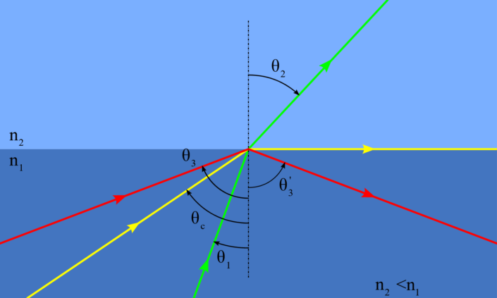
The most important principle for integrated photonics is total internal reflection. For a lot of people, “total internal reflection” sounds like something they might have been tested on in middle school and then promptly forgot about. It comes down to the speed of light when travelling in different materials. If the light has to cross to a different material, where it must travel more quickly, its direction will bend depending on the angle it enters the new material with. That bending of the light is called refraction. If that angle is shallow enough, it bounces back off completely. That’s total internal reflection. The beam of light is totally reflected on the edge of the material, and it continues its travel internally.
Depending on the angle that the light hits the interface between the two media, and the difference in light velocity between them, it can refract (green), travel across (yellow), or reflect back into the first medium (red).
If You Are Reading This…
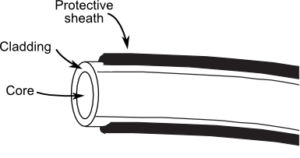
When the material is has the right properties, light can remain trapped within it and continue to propagate. The plastic on the left (PMMA) can do this due to light velocity within it being very different from its velocity in the air. Optical fibers such as the one on the right require a covering material, called cladding, to keep the light bouncing inside the core.
If you have high speed internet, you are using this principle. The ‘pipes’ we use to connect the billions of computers that make up the internet are called optical fibres, because they are strands that chaperone light. These optical fibers are one of the reasons the internet became much, much faster since the days of copper wire internet. Light and electricity are two sections of the electromagnetic wave spectrum, but light is a much bigger section.
As the frequency increases, the amount of transmittable information also increases. The right side of the spectrum is therefore much more dense than the left. Image is adapted from NASA.
The Smaller Picture
All these concepts are about photonics, the science and engineering of light. Where the ‘integrated’ part of integrated photonics comes in is when we take the cables that carry the light and make them very, very tiny.
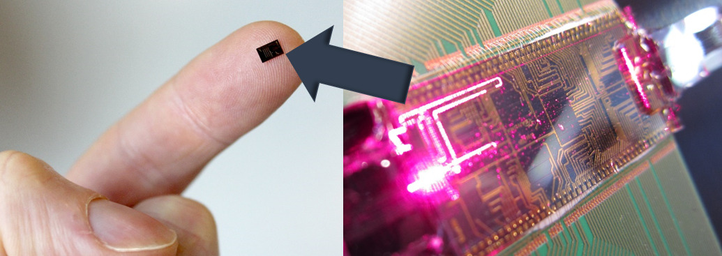
Photonic chips can be so small that they can fit on your fingertip with room to spare!
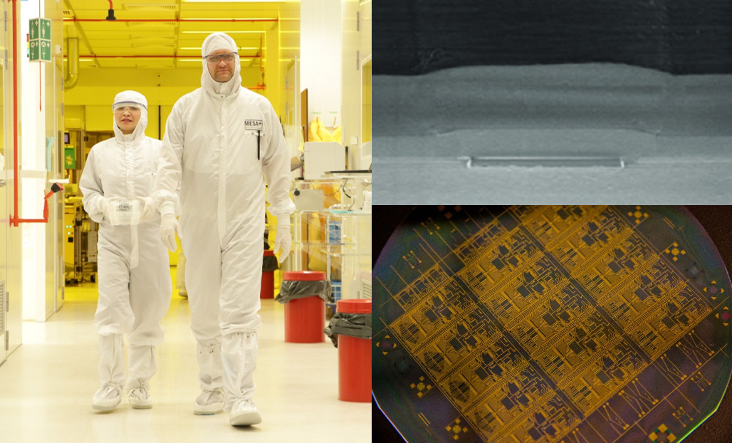
Instead of making a fiber and trapping the light in it, we make a tunnel inside of a chip and let the light travel through that. These trenches are about a thousand times narrower than human hairs. Making them requires specialised labs that actively suck any solid particles out of the air in them. Lab technicians have to wear bodysuits to trap any hairs or bits of dust floating off of their skin. The ground on which the labs are built have to be isolated from the vibrations travelling through the earth.
Our engineers work in specialized labs called cleanrooms (left), where they work on producing trenches of material that can carry light through a chip (top right). These trenches, called waveguides, make up the complex geometries that allow photonic chips to manipulate light in many different ways.
These photonic integrated chips can do way more than just transfer the light from one computer to another. It can generate and detect it, as well as change its properties, like its phase and frequency. Its name gives a hint as to what it can best be compared to: integrated circuits. Those are the more familiar electronic chips that do the processing work in computers and phones.
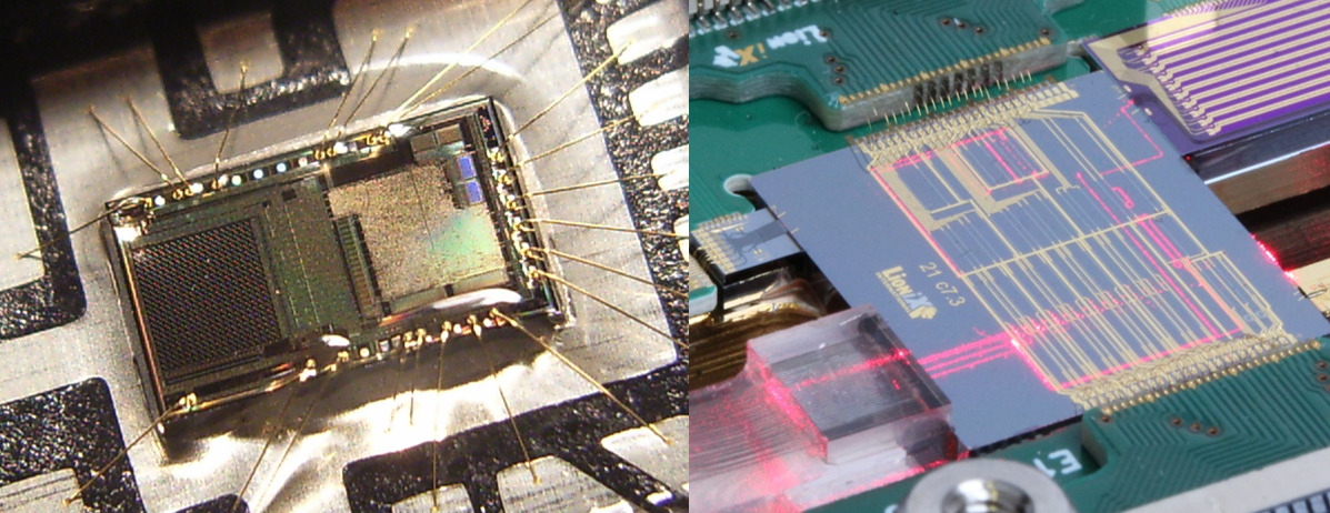
The different between an integrated circuit (left) and a photonic integrated circuit (right) can be subtle, but there’s always a tell: it’s the light.
There are many applications where a chip operating with light can outperform one working with electricity. Light can carry signals that are much more dense with information than electricity, so processing those signals in photonic chips is faster and more energy efficient than in electronic chips. Light is also more sensitive to environmental changes, so photonic chips can be used as sensors in biological applications as well as in quantum computing. Light can be used to make very responsive distance measurements at very high accuracies. The range of applications in which photonic integrated circuits shine are only increasing as integrated electronics reaches its optimal peak.
Tip of the Iceberg
Of course, these are only the highlights of what goes on at LioniX International and other photonics development companies and research groups. On the Day of Photonics, many of the firms working in this wide field take the opportunity to introduce the public to our exciting work. This year, we took to brainstorming new ways to communicate all this knowledge out to you. In our experience, the best brainstorming is done with the brain’s favourite fuel: sugar.
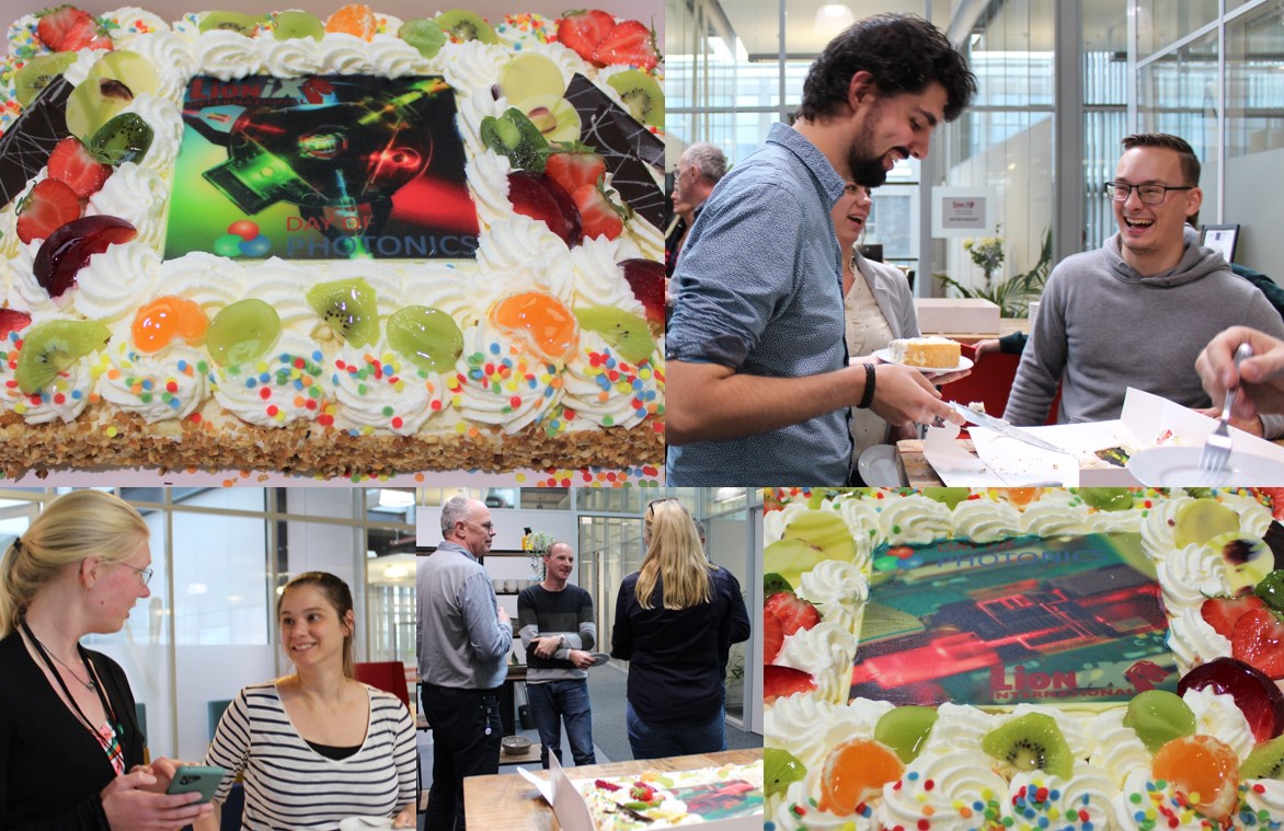
This is not even everyone at LioniX! But we made sure to save some for the rest.
Happy Day of Photonics and see you next year!

