On Chip Photonic Repeater for High Throughput Satellites
Despite the surge in wireless alternatives, satellite connections continue to play a crucial role in addressing challenges such as limited broadband coverage in areas with poor internet access – picture remote islands or ships navigating the open sea. They prove crucial in security-sensitive zones where cyber threats are too risky – satellites ensure secure communication channels for embassies or the military. In times of natural disasters causing damage to terrestrial networks, satellites serve as an essential alternative infrastructure. Thanks to High-throughput Satellites using Photonic Integrated Circuits, data transmission and communication through satellites can now be accomplished more efficiently and at reduced costs.
High-throughput satellites (HTS) are communication satellites that can handle and transmit a significantly higher amount of data compared to conventional fixed satellite services (FSS).
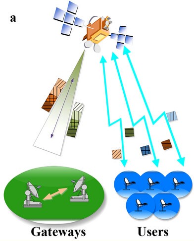
In conventional satellites, the forward links, or the communication links that go from the ground-based gateways up to the satellite and then down to the end users, are made of broad single beams that cover large geographical areas (as big as a continent). In contrast, HTSs use spotbeam technology, where the beams are narrow and cover much smaller geographical areas (hundreds of kilometers). For that reason, the same frequencies can be reused by different beams without interference – they cover non-adjacent geographical areas, and that increases the link capacity significantly. The capacity of an HTS can be 100 times higher than that of an FSS for the same available spectrum. Consequently, the cost is substantially reduced.
Figure 1: High-throughput satellites concept.
PICking it: Higher HTS flexibility through programmable photonics
Microwave integrated circuits (ICs) have long been the go-to technology for High Throughput Satellites, especially when developing radio frequency (RF) repeaters and transmitter-receiver modules. However, their adaptability to large-scale multiplexing and flexible signal processing is usually restricted by frequency constraints. A robust solution to this issue involves incorporating photonic integrated circuits (PICs). They not only allow a flexible implementation of HTS payloads but also offer the advantages of reconfigurability and potential multi-task operation. In comparison with microwave ICs, PICs bring in a large range of benefits such as flexibility, scalability, customization, and cost reduction to satellite payloads.
In HTSs, repeaters and signal processing are subject to specific requirements. One of the main features of HTS in orbit is that the radio frequency signals received by the forward link are eventually processed by analogue-to-digital convertors (ADCs), which typically have an analog bandwidth of 500 MHz. Therefore, the practical application of repeaters is to down-convert the high-frequency broadband signal into couples of intermediate frequency (IF) narrowband signals.
With PICs, these requirements can be easily accommodated. LioniX has designed, fabricated, and demonstrated several complete repeater systems for the next-generation HTS payloads. These systems comprise fully-packaged, hybrid-integrated, on-chip photonic RF repeaters as well as their control electronics. Photonic repeaters here are designed for the forward link, that is, the realization of broadband (2 GHz) to narrowband (500 MHz) communication links. On-chip functionalities include multi-channel signal modulation, frequency down-conversion, and photonic channelization , effortlessly realizing in-orbit switching.
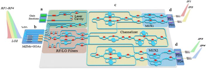
The schematic of the photonic repeater is provided in Figure 2. It shows the different functional parts of the repeater hybrid PIC. These parts belong to different chips realized on two different platforms: indium phosphide (InP) for the active functionalities and TriPleX® silicon nitride (SiN) for the passive functionalities. The InP gain sections are on; Mach-Zehnder modulator (MZMs) and semiconductor optical amplifiers (SOAs) are on the chip b; the laser cavity, the RF/LO filters, the channelizer, and the multiplexers (MUX1 and MUX2) are on the chip c; and the four photodetectors (PDs) and their corresponding trans-impedance amplifiers (TIAs) are on the chip d.
Figure 2: The schematic of the photonic repeater.
The principle of operation of this repeater is explained as follows. A broadband signal (RF1-RF4) from the gateway beams is modulated by one branch of internal carriers of the photonic RF repeater. Meanwhile, two optical local oscillators (LOs) with different frequencies are generated parallel to the RF branch. Then, an SOA array and a broadband filter array are employed for gain compensation and spurious suppression, respectively. Regarding the LO branches, two equal-power dividers enable separating LO signals into four parts. In terms of the RF branch, a channelization module is followed by a broadband filter, resulting in four channelized signals. Finally, four pairs of channelized RF signals and LO signals are fed to a set of optical combiners for on-chip frequency down-conversion through optical heterodyning in the PDs.
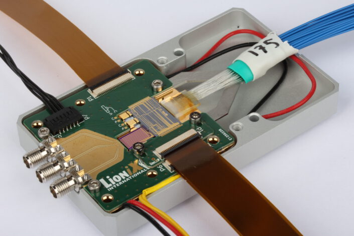
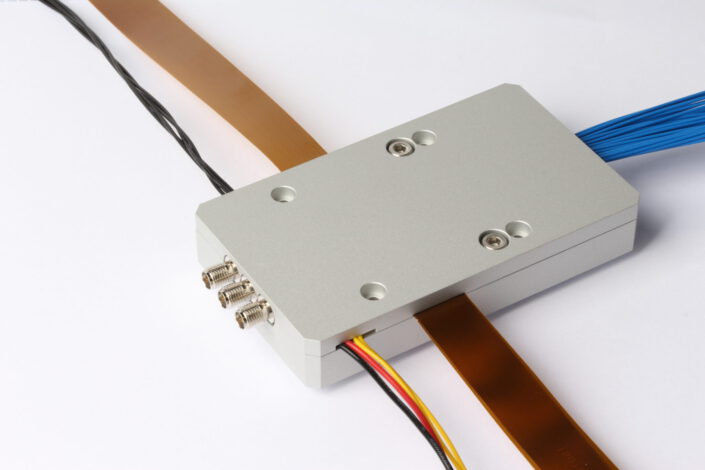
In addition to designing and fabricating the TriPleX® chips for the repeater module, LioniX assembled the InP chips around TriPleX® to create the hybrid assembly. Moreover, we designed a printed circuit board (PCB) and wire-bonded it to the hybrid assembly. Further, LioniX designed the packaging for the assembly, as well as the driving electronics to control and tune the module. Figure 3 shows photos of the repeater module with the package open and closed.
Figure 3: Photos of the repeater module with the package open and with the package closed.
Putting it to the test: How well did the photonic repeater perform?
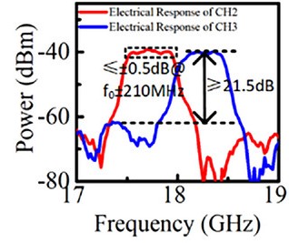
Together with our in-house control electronics development, LioniX also developed software tools with a graphical user interface to characterize and tune all the actuators and functional blocks in the repeater module. The module is also equipped with optical fibers, which was used to tune and monitor the response of the functional blocks. Further and finer tuning was achieved with the electrical spectrum analyzer and the vector network analyzer. An example measurement of the electrical response of CH2 and CH3 is shown in Figure 4. The flatness of the 420 MHz passband is ≈ 0.5 dB, and the out-band rejection is > 21 dB.
Figure 4: demonstration of the channelization concept.
First, the repeater module was tuned such that it passes only one RF band centered at 26.8 GHz to its fourth output, and down-convert it to 17.5 GHz. Then, a QPSK signal of 32M Symbol/second was generated at 2 GHz then up-converted to 27 GHz by a 25 GHz mixer LO before being applied to the RF port of the repeater module. The EVM at the input of the repeater module was measured at 5.4%.
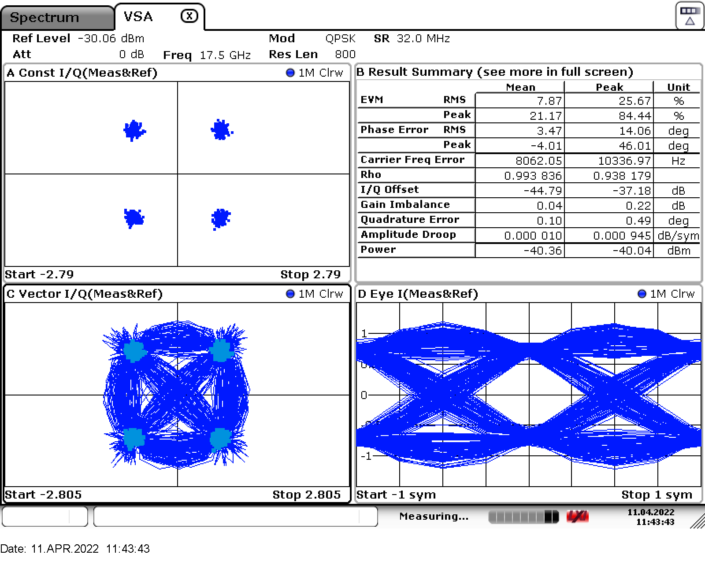
This signal was applied to the RF port of repeater module. Then, the repeater module successfully down-converted the data signal to 17.5 GHz. The down-converted data signal was detected by a vector signal analyzer (VSA), which displayed the signal constellation, trajectory, the eye-diagram of the I-data signal, and the measured EVM (7.9%) for the received signal, as shown in Figure 5.
The experiment was repeated five times at different center frequencies that are separated by 100 MHz. That is, at 26.6, 26.7, 26.8, 26.9, 27.0, and 27.1 GHz. The corresponding measured EVMs were 8.9%, 10.0%, 7.9%, 6.4%, 7.1%, and 9.0%, respectively. This proved that the 32M symbol/second is a limitation from the measurement equipment (VSA) rather than the repeater module itself.
Figure 5: Demonstration of data transmission via the repeater module.
Smaller, lighter, more efficient: the integrated photonic advantage in HTS payloads
Compared with the traditional HTS payloads architecture based on microwave technology and the photonic HTS payloads architecture based on discrete optical modules, the photonic integrated payloads solution can achieve a higher level of integration of RF front-end processing. This new photonic architecture can greatly improve the flexibility and scalability of HTS communication payloads. of a high-throughput signal processing payload achieved by full-chip photonic RF repeaters. Moreover, the core functions, such as RF channelization, show outstanding performance compared with corresponding discrete products. Such synergy of multifunction chips toward complicated on-orbit signal processing is an essential step for the next generation of fully integrated HTS payload.

Dr. Ahmad Mohammad received the joint M.Sc. degree in photonic networks engineering from Aston University, Birmingham, U.K., and Scuola Superiore Sant’Anna, Italy, in 2015, within the European Erasmus Mundus Program. Then, he joined the Ultra-Fast Photonics Group at University College London (UCL), as a Marie-Curie Early-Stage Researcher within the H2020 FiWiN5G project, where he also received his Ph.D. degree in integrated photonics for millimeter wave transmitters and receivers in 2019. Since then, he has been working at LioniX, as a projects leader in the Microwave Photonics Systems department.
Take a look at:
🌐 The academic paper on which this article is based.
🌐 An article about Integrated photonics modules for better synthetic aperture radars.
🌐Microwave photonics development at LioniX International.
🌐 Our newsletter, with monthly updates on our developments and events.

