Impressive compression: TriPleX® integrated photonics for image processing
Tom Horner, 01 September 2021
A group of researchers based at the Instituto de Telecomunicações in Portugal have used LioniX International technology to build a photonic integrated circuit (PIC) that drastically compresses image data. The chip-based technology reduces storage capacity and transmission bandwidth requirements for imaging systems. It could even be deployed in a signal line directly from a camera to reduce latency for real-time object recognition.
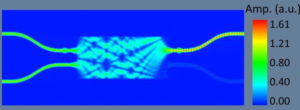
Fig. 1: The amplitude of the light field as it propagates through the optical building block designed by the team
Smarter imaging systems
Advances in imaging and communications technology have given us deeper insights into important systems in medicine and the environment. Besides higher resolution, improved image processors now offer powerful automation and smart object recognition.
However, despite advances in network speeds and storage capacity, high resolution image data is still burdensome to transmit and store. Furthermore, as technology has advanced, so have demands. Users expect real time insights from pre-processed image data, exerting pressure on systems developers to reduce latency.
Low-loss waveguides for performance and scalability
The chip fabricated by the Portuguese research team addresses network and storage pressures by automatically stripping out redundant image data. The results are impressive; in a recent paper1, the researchers reported a compression rate of 75% for an array of pixels. Their chip used integrated photonics (comprised of multimode interference structures and phase modulators) to transform optical signals so as to identify and remove information that was not useful for image recognition.
Whilst initially implemented for a one-dimensional green pixel array, the principle also holds promise for two-dimensional, full-spectrum image processing. Working with optical signals in this way removes the need for conversion between optical and electrical domains, opening up the possibility for very low latency signal processing.
Here, TriPleX® waveguides fit the application perfectly. Not only do the components benefit from the very low propagation losses of TriPleX®, but the broad transparency of silicon nitride waveguides supports full-spectrum image processing capability.
Furthermore, the chip designers were able to use the ideal confinement of light in TriPleX® to create tightly spaced components and reduce device footprint, down to 4.7 times smaller than with other integrated photonic platforms.
Beyond the specific value of TriPleX® waveguides, photonic integrated circuits (PICs) enable other commercially important capabilities. Firstly, PICs are small and robust compared to systems built from separate optical components. They are also scalable. Manufactured using batch processes on semiconductor substrates, PIC production can easily be scaled for higher volumes and lower costs per device.
Towards 2d image processing
The team’s achievements show the value of optical image compression and the capabilities of TriPleX® chips. Their next challenge is to further reduce optical losses and move towards full image processing. Here TriPleX®, with its low-loss light coupling through easy spot size conversion, looks set to pave the way for more exciting developments.
- A. Fashi, M. H. V. Samiei, C. Pinho and A. L. Teixeira, “Photonic Integrated Chip on TriPleX Platform for Realizing Optical Haar Transform and Compression in the Visible Spectrum,” in IEEE Journal of Quantum Electronics, vol. 57, no. 5, pp. 1-10, Oct. 2021, Art no. 6300210, doi: 10.1109/JQE.2021.3102845.
https://ieeexplore.ieee.org/document/9507454


