MEMS Technology

With over 20 years of experience in microsystems fabrication using MEMS technologies, we have developed a valuable array of technologies designed to realize your MEMS device. Deep reactive ion etching and and wafer bonding are key amongst these vital enabling technologies.

Through continual development in our state of the art cleanroom we have refined existing technologies and continue to develop new custom capabilities in partnership with our customers.

You will find an overview of all of our most important MEMS technologies and building blocks below.

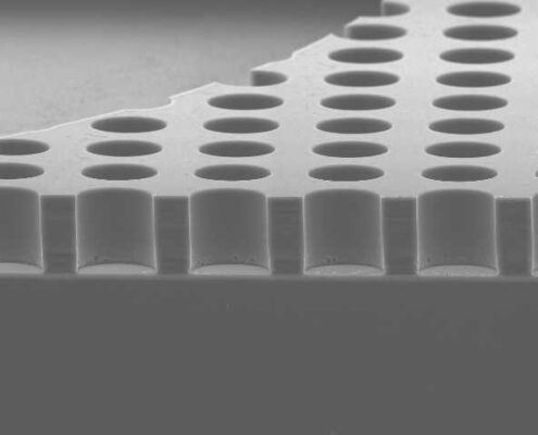
scanning electron microscope image (SEM) image of a silicon on insulator SOI MEMS

Silicon on Insulator Wafers (SOI) Processing

Silicon on insulator wafers (SOI wafers) offer excellent performance for advanced MEMS devices. Our SOI processing includes deep reactive ion etching, release etch, bonding and etch back and trench fill process.
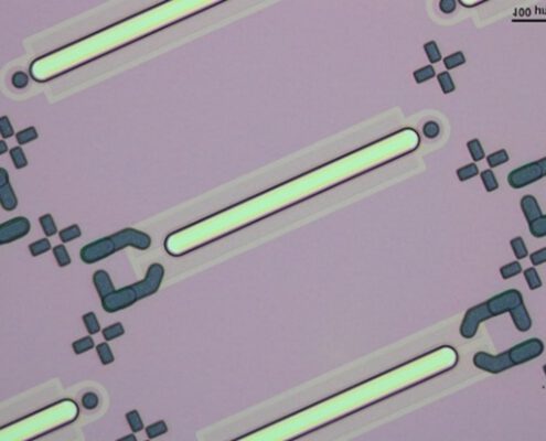
An image of a component layout on MEMS pH meter based on custom ISFET made by LioniX International.

Ion Sensitive Field-Effect Transistor (ISFET)

Welcome to The ISFET Factory! Our ISFET bare dies with Tantalum Oxide (Ta2O5) gates are an excellent base for your pH- or ion sensing system.
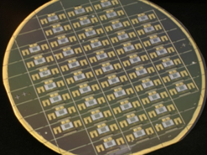
Photo of a packaged wafer made by LioniX International

Wafer Level Packaging of MEMS

We use a plurality of wafer bonding techniques to protect your MEMS against mechanical and other environmental influences.