Visible Light Multi Project Wafer Services
Our multi project wafer (MPW) services give you access to visible light applications using the uniquely broad transparency range of our silicon nitride technology. This MPW service is optimized for low loss integration with optical fibers using low contrast waveguides.
Optimized for visible light, this multi project wafer service enables the integration and miniaturization of systems for life sciences, such as fluorescence microscopy, which have typically relied on visible light for imaging. Other users find visible light beneficial for its relatively high energy and strong interaction with materials. Applications include optical phased arrays, image processing, and optical interferometry for telescopes. Visible light photonic integrated circuits (PICs) make for compact, robust, and power efficient devices for the same purposes.
Visible Light Multi Project Wafer Benefits
- Silicon nitride waveguides optimized for low loss transmission of visible light
- Ideal for integration with visible light sources
- Enable on-chip processing of imaging information
- Higher component density with relatively short wavelength light
How To Use Our Visible Light MPW Service
Review the visible light MPW schedule to plan your project, then contact us to arrange the details! Our visible light MPW process design kit is available for various design software, including Nazca, OptoDesigner, and IPKISS.
Visible Light Photonic Integrated Circuits Applications
Our visible light MPW service offers a PDK with standard building blocks as well as allow for new designs to be implemented on our TriPleX® platform. The service has enabled researchers to produce innovative photonic devices at a budget. Here are a few examples of visible light silicon nitride PICs.
On-Chip Spectrometry
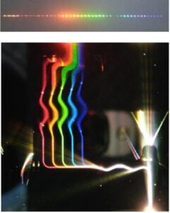
Visible light photonic integrated circuits have been deployed in spectrometry, as in the EU-funded project InSPECT. The project aimed for the development of an integrated spectrometer for optical tissue characterization. The characterization method, known as Diffuse Reflectance Spectroscopy, uses a broadband light source to illuminate a tissue sample. The tissue scatters light at wavelengths characteristic of the tissue type and its condition. To identify this response regardless of tissue type and possible condition, the collection of a broad spectrum of light and its subsequent separation is required. This was achieved using arrayed-waveguide gratings (AWGs), which is a standard building block included in our visible light MPW process design kit. Each AWG separated the input light into its component wavelengths. By cascading multiple AWGs, the scattered light was separated into increasingly narrow wavebands, each carrying a specific section of the spectrum. The device ended in 50 light channels, which were hybrid-integrated with dedicated photodetectors.
A TriPleX® visible light chip with arrayed waveguide gratings for spectrometry. Top panel shows the output facet, with the full spectrum light split into multiple channels.
Novel Photonic Devices from Basic Building Blocks
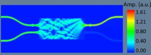
Researchers at the Instituto de Telecomunicações in Portugal designed a composite building block in TriPleX® for image processing, based on a multimode interferometer, phase shifters, and splitters.
The novel circuit carried out an all-optical Haar transform, which is used for fast, real-time image data processing and compression. Such tasks are typically handled by electronic devices which expend a lot of processing power on the ballooning data demands of high-resolution images and real-time communication. Offloading such tasks to photonic chips frees up computational resources for other tasks. This approach is also faster, as it circumvents the need to convert the image data from the optical to electrical domains for processing then back to the optical domain for transfer.
In the MPW chip, seven circuits with variations on the design were fabricated to test out different geometries and differences in the performance of TE and TM modes. The TriPleX® circuit achieved a 75% compression rate for an 8-pixel array at 532 nm light, with the possibility of full-spectrum image processing using the platform’s wide transparency.
Light propagating through a TriPleX® visible light MPW chip designed by the researchers to carry out the Haar transform for image processing.
Interferometric imaging with Silicon Nitride PICs
Modern astronomy utilizes optical interferometry to combine the light gathered via multiple telescopes, forming a meta-telescope out of an array of telescopes with a diameter equivalent to the distance between the farthest two telescopes in the group. This approach creates composite images with high angular resolutions, and is already being used at the Center of High Angular Resolution Astronomy and will be deployed in the Square Kilometer Array Observatory. Crucial to the operation of such interfermetric telescopes is the use of beamforming systems to compensate for optical path differences between the subject of observation and the point of light collection.
Through the advances of microwave photonics, such optical beamformers are possible to integrate on chip. Researchers at University of California and Lockheed Martin demonstrated a small-scale Fourier-domain interferometric imaging telescope that used silicon nitride PICs to detect white-light interference fringes. The device combined the light of two inputs using basic photonic chip building blocks, including multi-mode interferometers and arrayed waveguide gratings. Such devices make great strides towards making modern astronomy smaller, smarter, and more power efficient.


